
Electronics & Semiconductor cover — CNC machining services

Industry

Electronics & Semiconductor Industry Solutions

CNC Machining · Rapid Prototyping · Assembly

96.9%
Perfect orders
100M+
Parts manufactured
60+
Industries served
5 days
Avg. prototype turnaround

For wafer handling, vacuum chambers, optics stages and test equipment — high-tolerance parts with the cleanliness and documentation chain your ISO Class 3 cleanroom audits demand, from first article through 100k+ annual volume.

Applications

What we make for electronic & semiconductor

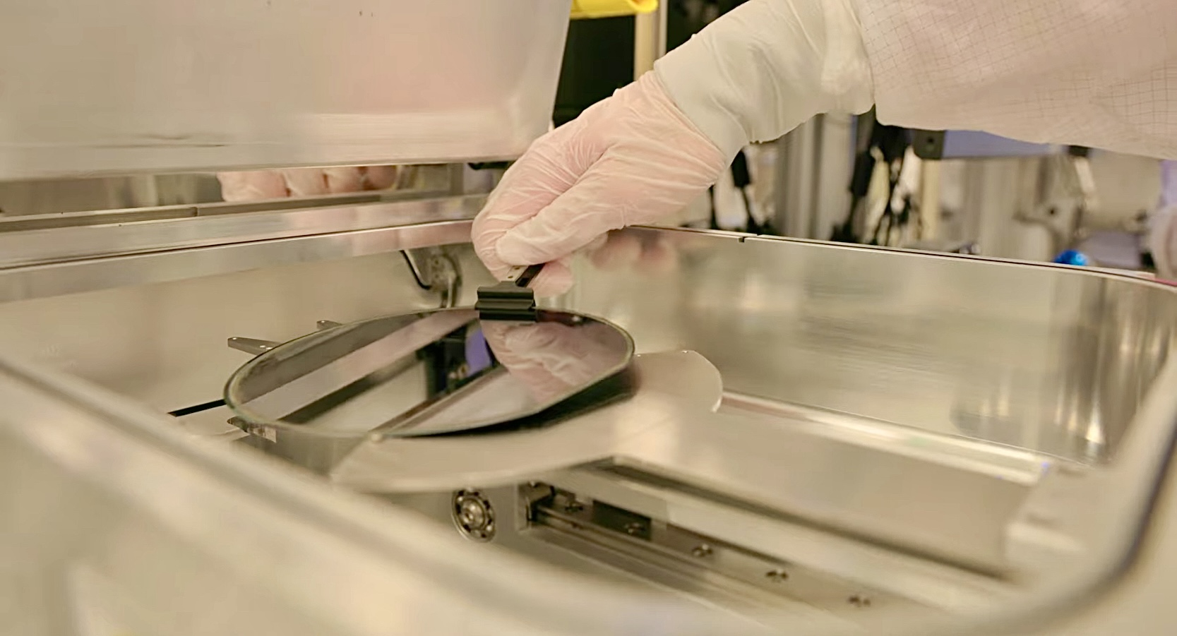
Wafer-handling gripper body in stainless

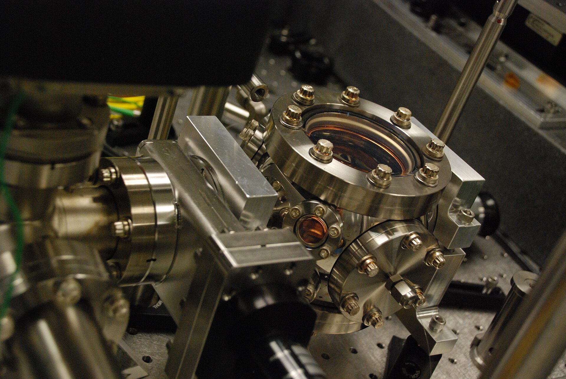
Wafer-Handling & Vacuum Chambers

Bernoulli gripper bodies, edge-grip fingers, vacuum chamber doors, viewports and ISO/NW flange adapters — machined in 316L VAR stainless and electropolished to Ra 0.4 µm on sealing faces. Helium leak testing is available on every vacuum-rated part (test sensitivity: 1×10⁻⁹ mbar·l/s). Each lot ships double-bagged with full lot traceability for ISO Class 3 cleanroom delivery, including material certs (ASTM A276/A479), surface-finish readings (profilometer), and CMM report on first articles. We machine to ±0.01 mm on all critical sealing and dowel features, with vacuum-bake pre-treatment available for outgassing-critical applications.

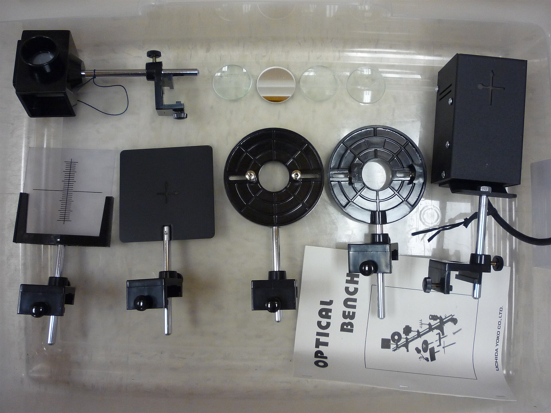
Precision optics mount and kinematic base

Optics & Test Fixtures

Optics mounts, kinematic bases, flexure components, probe-card stiffeners and alignment jigs for semiconductor ATE and precision optical systems. These parts cannot deflect under their own load — we hit ±0.005 mm on critical locating features and ±0.01 mm on dowel alignment holes, with full first-article and CMM reports. For thermally sensitive applications we specify Zerodur or superinvar (CTE < 0.1 ppm/°C). All aluminum parts receive Type III hardcoat anodizing for wear resistance, and we can apply vacuum-deposited aluminum coatings for reflectivity-critical surfaces. Typical surface finish on optics-contact faces: Ra 0.4 µm or better.

Process gas showerhead plate

Process Gas & Fluid Handling

Stainless process gas lines, VCR fittings, showerhead plates and valve bodies for etch and deposition tools (ALE, CVD, PVD, ALD). Built from traceable 316L bar stock (ASTM A276, VAR grade) with dimensionally inspected and cleaned-to-spec documentation structured to drop straight into your FAI package. All wetted surfaces are electropolished and particle-count tested (per SEMI E49) before packaging. Common specs: ±0.025 mm on flow-channel dimensions, Ra < 0.8 µm on interior surfaces. We also machine precision orifices and restrictors to ±0.005 mm with flow-coefficient testing on request.

PCB assembly precision jigs and stencil frames

PCB Assembly Equipment

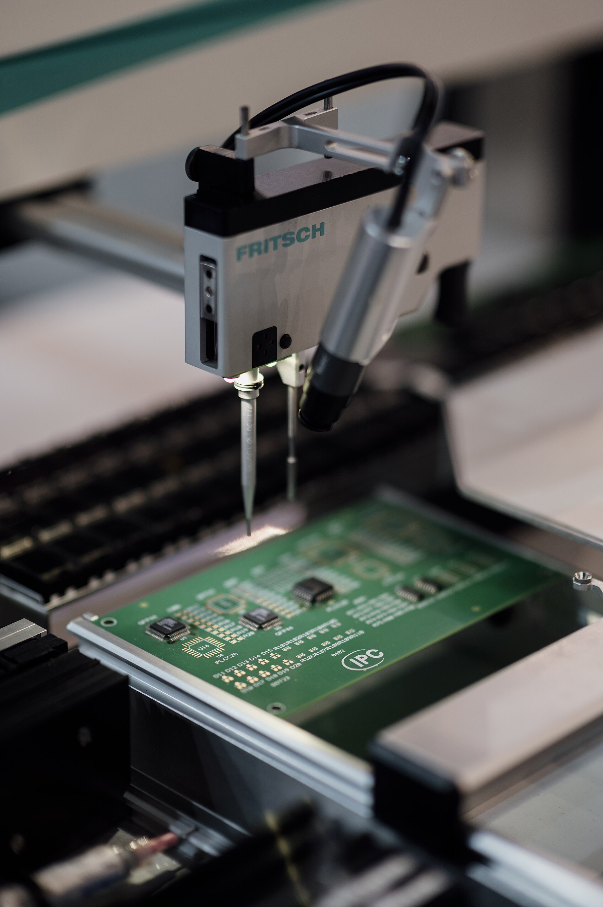
Nozzle nests, carrier frames, solder-paste stencil frames and precision-machined jigs for PCB assembly lines (SMT, THT, selective solder). We work in 6061-T6 aluminum and 316L stainless with tolerances from ±0.02 mm on non-critical features down to ±0.005 mm on critical locators. Anodized and hardcoated finishes resist solder flux and extend tool life in high-volume production environments. Common features: vacuum-chuck flats held to ±0.01 mm flatness, precision-indexed fiducial plates for optical recognition systems, and anti-static (ESD-safe) surface treatments. We can also machine custom stencil frames to any panel size with frame-weld flatness guaranteed to ±0.05 mm.

Semiconductor IC packaging components

Semiconductor Packaging

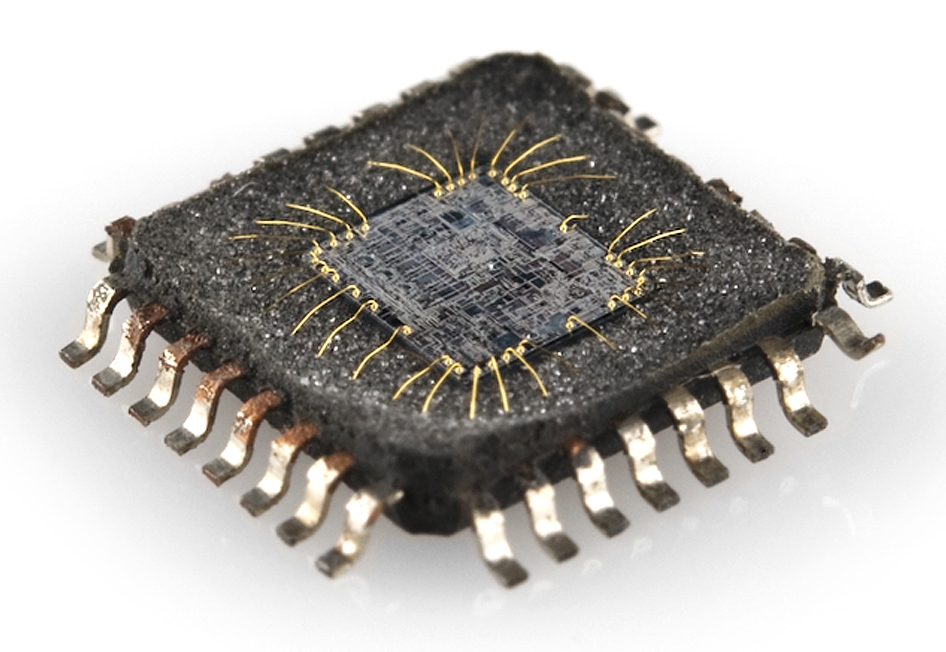
Clip-frame packages, leadframe carriers, clip-bond heat spreaders and ceramic substrate clamping plates for IC packaging (QFN, BGA, flip-chip, fan-out wafer-level). We machine in copper-molybdenum (CuMo), copper-tungsten (CuW), alumina (Al₂O₃) and aluminum nitride (AlN), holding ±0.005 mm on thermal-interface feature dimensions. Thermal conductivity specifications are met through certified material supply with mill certificates. Surface finishes range from as-machined to gold-plated (1.27 µm min) for solderability-critical applications. All parts ship with material certs, dimensional report and, where specified, thermal-resistance testing data.

Probe card stiffener and test hardware

Probe Card & Test Hardware

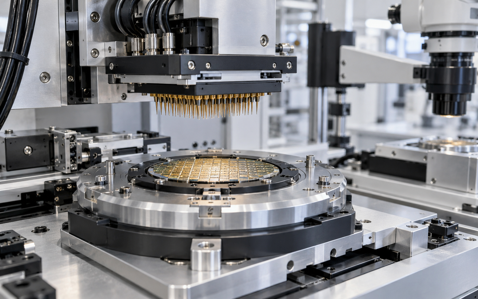
Probe card stiffeners, membrane supports, DUT (device-under-test) clamping plates and thermal-test chucks for wafer-level test and burn-in. These components must maintain flatness under thermal load — we specify ±0.005 mm on probe-contact features and hold flatness to < 0.025 mm/m on thermal-chuck surfaces across the operating range (-55 °C to +150 °C). Materials: 316L stainless, invar for low-CTE applications, and aluminum 7075-T6 for thermal-chuck bodies. We coordinate with your probe-card integrator on datum schemes and contact-pitch requirements, and we can provide first-article CMM reports with thermal-cycled re-measurement data.

How we work

Materials, tolerances, collaboration

Semiconductor capital equipment and high-end electronics punish anything that drifts out of spec. Wafer-handling arms swing through 10 million cycles a year; vacuum chambers cannot outgas; optics stages cannot deflect under their own load. We machine for that environment — and we know the audit trail it demands, from raw-material lot number through final package inspection.

Materials and tolerances

For vacuum and cleanroom service we default to 316L VAR-grade stainless, electropolished to Ra 0.4 µm on sealing faces. Aluminum 7075 handles structural pieces where weight matters. We routinely hit ±0.005 mm on critical locating features and ±0.01 mm on through-holes for dowel alignment. For ultra-stable optics stages we work in Zerodur and superinvar when the thermal coefficient of expansion is the governing spec, and we can hold CTE-matched assemblies across the operating temperature range.

Cleanliness and documentation

Parts ship double-bagged with lot-level traceability. Each batch is accompanied by material certs, surface-finish readings, and a CMM report on first articles. When your installation needs ISO Class 3 cleanroom compatibility, we adjust packaging and cleaning to match. We can also perform residual particle counts (per ISO 14644) and Helium leak testing on vacuum components before shipping.

Traceability chain

From raw-material lot number through machined part, first-article inspection and packaging — every step is documented in a traveler that drops into your FAI package. For fab-tool suppliers we support SECS/GEM data collection, including in-process measurement logging and tool-offset records. We maintain a 10-year document archive per project so your procurement team can re-order without re-qualification.

Custom Machined

Custom Machined Your Electronic & Semiconductor Components

With an extensive history in prototyping electronic & semiconductor components, we bring a wealth of knowledge and expertise to every project. Send the CAD and the target outcome — engineering will reply with a focused quote within one business day, routed to the cell most familiar with this vertical.

Get a free quote